PH Series Thru-Hole Connectors from JST

TLDR; make your plated thru-holes 0.8mm diameter for these components.

Long Version:

Many of our customers like using your PH series connectors on their circuit boards. According to page 1 of JST’s datasheet, these holes are recommended to be 0.7mm diameter plated-thru-holes.

PH series connector from JST with bent legs

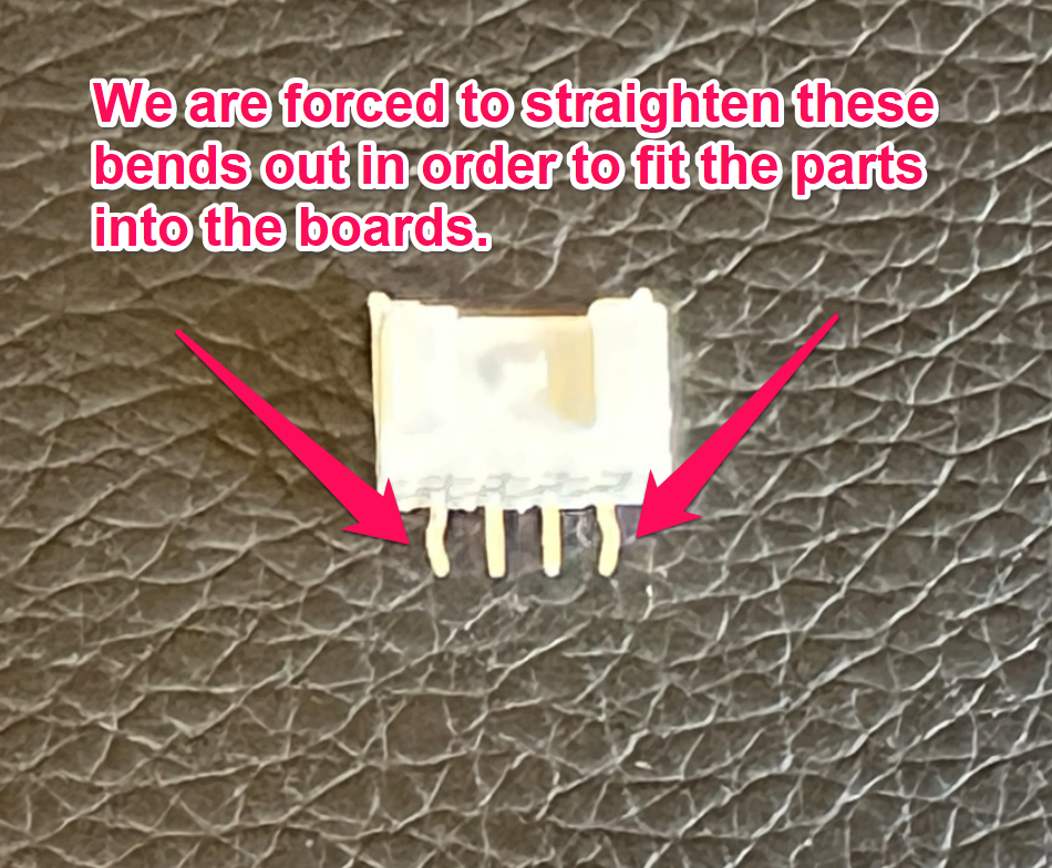
The trouble is, this hole is too small for the bent outside pins of these connectors. When they get bent, they do not fit into the hole and we find ourselves having to use pliers to squeeze this bend away and make it straight in order to get it into the hole. If we don’t, we end up with either very sore thumbs or damaged components, and oftentimes both.

 
PH connector JST no negative tolerance

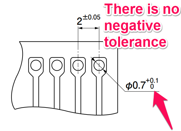
If you look closely, you will notice that JST has provided a positive tolerance of 0.1mm but no negative tolerance. Pretty much every PCB fabricator we have ever worked with has told us that they have a +/- tolerance of 0.1mm for plated-thru-holes. Meaning boards designed with a 0.7mm diameter hole will end up with holes as small as 0.6mm and as large as 0.8mm and still be within their manufacturing tolerance.


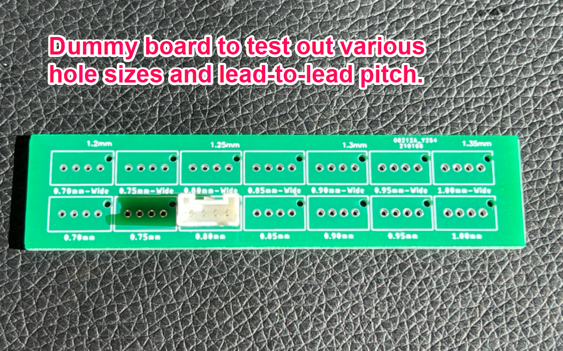
We went so far as to create a dummy board to evaluate the best size to make these holes for repeatable results. We've found that making these holes 0.8mm means that we can properly assemble boards without removing the bend on the outside leads of the component.

PH Connector JST Dummy Board

So for the sake of all of our sore thumbs, please adjust your footprint libraries to make these 0.8mm plated thru-holes :)

Solder mask dams between fine pitch devices

There is a virus running through this world, threatening to destroy all quality circuit boards. As devices get smaller and smaller and pitches get tinnier and tinnier, more and more board fabricators are taking the easy road out and refusing to put solder mask dams between the copper pads of fine pitch devices. We must end this virus in its tracks before it threatens the entire eco-system of manufacturable boards!

When designing products with 0.5mm or even 0.4mm pitch QFP and QFN style devices, please use the following design rules. Then please insist with your PCB fab to meet these design requirements. They may not like it, but they’re fully capable of producing it.

When designing for a 0.5mm pitch device, please use this copper width and this mask width.

The PCB fab will want to have at least 0.1mm gap between the mask opening to create a solder mask dam

The PCB fab will want to have at least 0.1mm gap between the mask opening to create a solder mask dam

Component Supply Shortage: Using Non-Authorized Vendors

Worthington Assembly has always made a point to source electronic components from authorized distribution channels (the Digi-Key, Mouser, Arrow and Avnets of the world); however, recently many of our customers have begun to see notes referencing specific BOM lines being quoted from non-authorized vendors on quotes that we provide.

Due to the current global semiconductor shortage we have been needing to branch out our supply chain to be able to quote and secure the components required on almost every job that we are quoting these days. This means quoting components very often at high markup from "non-authorized" resellers. This designation simply means that these companies (Winsource Electronics, Quest Components, and LCSC being among the most common NA vendors we use) do not have the authorization of the manufacturer to resell these parts, and are not franchised distributors.

Very often these companies seek out high risk inventory and purchase large quantities either directly from the manufacturer or from authorized-vendors, and then resell the parts at a very high markup. They exploit the market conditions and make a lot of money doing it because very often they clean out the global inventory leaving our customers either facing a 52+ week lead time or a redesign.

In addition to non-authorized resellers, there are also brokers -- they are technically non-authorized as well, but they don't operate the same way. They mainly work on a component request basis to secure inventory for a given order for a customer. They might get an email from us asking if they have access to a given part and then contact another Contract Manufacturer to see if they have some of these on the shelf sitting unused that they could sell to the broker to in turn, markup and sell to us to fulfill our needs.

We list these for approval specifically on our quotes because we cannot warranty the parts themselves. They may not be traceable and they may not have CoC's -- the only thing that we can guarantee is the quality of the work that we perform (ie. the quality of the solder joints in accordance with IPC and the process by which we assemble the boards to spec in the prints or files provided).

That being said, in the last 6+ years, we can recall only a single instance of us getting a part that flat out didn't work and *may have* been fraudulent. If we ran into an issue where a customer believed the parts were the problem we would do everything we could to work with them to get the boards working, but we need to be honest in letting our customer base know that this would come at a cost, and that labor charges for rework would apply. Importantly, there may not be another source to get those parts anyhow.

If you receive a quote back from our quoting team and see a note referencing a non-authorized vendor and do not feel comfortable assuming that risk please let us know. We may request that you provide a suitable alternate that is available through authorized channels so that we can revise the BOM and quote accordingly, or if you have stock on hand that you have secured ahead of time always feel free to provide these parts to us on consignment and we will remove the cost associated with the parts from our quote.

If you have any further questions, please feel free to reach out to the author of this blog post at bbabilonia@worthingtonassembly.com

Press Fit Design and Assembly

Press fit connectors and pins have become increasingly popular recently, for a variety of reasons. Rather than repeat these reasons, which can easily be found with a quick search of the internet, let’s discuss the design and assembly challenges associated with press fit parts.

Design

In order for the assembly of a press fit component to be successful, it must first be designed for success. This starts with something as simple as defining that an area of your PCB will have a press fit connector installed in it. Why is this necessary? Because when it comes to press fit components, a tighter tolerance must be achieved with the plated-thru-holes in order to achieve the appropriate contact with the mating press fit pins. Think about it, if these holes were too large, and there was no solder holding them in place, then the pins could potentially slide out of their holes after repeated thermal cycles or mechanical stress from daily use.

The best way to communicate this requirement is to add this information in an extra layer of your design and then make sure to export that layer along with your other gerber data before sending it to us. This will help inform the PCB fab to pay special attention to this region to make sure that the tolerance of the drill is held precisely.

Additionally, when designing your circuit board, you need to make sure there is sufficient clearance around the press fit part to allow an anvil to be pushed up against the bottom of the PCB where the component is. If there is some kind of tall SMT component nearby, it might be impossible to get an anvil to fit properly without coming into contact and thus destroying this nearby SMT component.

Finally, you’ll want to double-check the footprint design your using to make sure it meets the requirements of the manufacturer of the component. Some manufacturers might require multiple layers of annular rings of copper in order to properly support the inserted pins.

Assembly

The press fit assembly process can be extremely destructive. If the proper tooling is not in place, it’s not uncommon to destroy the PCB in the press fit process.

Press

To begin with you will need to make sure you have a press with enough height clearance to handle the press fit component. Some press fit connectors are very tall and may not be compatible with basic arbor presses. Some connectors are very large and require significantly larger presses, so it’s always good to check with your manufacturer ahead of time to make sure they have the appropriate equipment for the application.

Press Head

If the component does fit the press you’re using, then you will need to make sure to have the appropriate press head for pushing against the component. Some components can be pushed with a flat piece of steel, whereas other components may need a special press head supplied by the manufacturer. Usually this will be defined in the manufacturers datasheet.

Press head designed specifically for its associated component

Press head designed specifically for its associated component

Anvil

Arguably the most important aspect of the press fit process is the anvil. When you press this component in place it is going to want to blow out the bottom of the PCB and destroy the entire assembly. Typically, without a proper anvil you will either not press the pins all the way in completely, because you’re supporting the entire bottom side of the PCB with a flat piece of steel, or you will destroy the PCB because you’re only holding the outside of the PCB up with some simple tooling pins or other standoffs.

The anvil is usually not supplied by the manufacturer of the component (unlike the press head). This means it will need to be custom engineered for your specific PCB design. Most shops that specialize in PCB tooling can help you with this design. Or you can request your assembly shop to work with a tooling specialist to get this designed and made for you.

Tooling

Finally, you need to make sure that the circuit board, the component, and the anvil all line up with each other properly, and repeatably, in order to achieve consistent results and get a high yield. This is usually accomplished with custom tooling that’s designed for your specific assembly. It will hold the PCB in place while the pressing operation is performed. It’s actually quite common to integrate the anvil into this custom tooling, but not always. Depending on the application you can sometimes get by with just an anvil, but this should be reviewed by the engineering staff at your assembly shop.

Tooling designed specifically for the PCB that gets the press fit component

Tooling designed specifically for the PCB that gets the press fit component

If your next PCB design will require press fit components, please reach out to us ahead of time before placing an order for a design review. This will help prevent any sort of frustration later on in case the design of the assembly is incompatible with the requirements of the press fit process.

If you have any questions at all, please reach out to us at info@worthingtonassembly.com or you may email the author of this article at cdenney@worthingtonassembly.com.

Recessing Your PCB Edge for Perforated Tabs (mouse bites)

Circuit boards do not exist in a vacuum. They're used in products and those products have other requirements that the board needs to accommodate. A lot of times these circuit boards have a specific shape that allows them to be fixtured either against another circuit board, a bracket, the edge of an enclosure, or something else, and the edge of this circuit board needs to be exactly correct for the final assembly to work. For most circuit boards a small amount of tolerance for the edge of the PCB is acceptable and can be accounted for. But sometimes it needs to be exactly right.

For those situations many customers prefer to have their PCB's "tab-routed" instead of "v-scored". A quick lesson in what "tab-routed" and "v-score" means is probably necessary.

V-Scored

Figure A - An example of a v-scored panel

Figure A - An example of a v-scored panel

A v-scored PCB means that when the individual PCB’s are put into a panel for automated assembly, a small v-shaped groove is cut into the top and bottom of the PCB along its edge (See Figure A). This makes it possible to break these PCB’s apart (depanelize) after the automated assembly process is finished. This v-scoring method has been used for many years and is the most inexpensive option for production work. V-Scores can only be placed along straight edges of PCB’s, so any curve to the PCB will have to be routed.

Figure B - Close up view of the v-groove

Figure B - Close up view of the v-groove

V-Scored PCB’s tend to leave a bit of a rough edge after they are separated from each other. Of course, roughness is relative because some may find it perfectly acceptable for their application whereas others might find it entirely unusable. Unfortunately there’s only one way to know for sure whether or not it will work for your application, and that’s to order some PCB’s that are v-scored and see if they’ll work for you.

There’s a number of ways to separate v-scored PCB’s. The easiest and simplest way is to simply snap them apart using your bare hands. The trouble with this method is that oftentimes small bits of the fiberglass will hang onto each edge of the adjacent PCB’s and create long string-like fibers. Usually just taking a piece of scrap PCB and rubbing it along the edge will clean up these fibers and smooth the edge down a bit. But a better way to separate these v-scored PCB’s is to use a tool specifically designed for such a purpose. Worthington Assembly utilizes a number of cab’s Maestro 3E tools for just this purpose.

Figure C - A popular v-score depanelizer

Figure C - A popular v-score depanelizer

The Maestro 3E has a sharp long knife on the bottom where the bottom v-groove rests, while a round blade is drawn across the top v-groove. The force of the two blades cutting through this v-groove separates the two adjacent PCB’s and results in a clean if somewhat rough edge. How rough? Well, that’s going to be different for each person. Some might find it perfectly smooth whereas others might find it completely unacceptable. The only way to know for sure is to order some for yourself and see how they turn out.

Tab-Routed

Figure D - An example of a tab-routed panel

Figure D - An example of a tab-routed panel

Tab-routing a PCB means that when the individual PCB’s are put into a panel for automated assembly, a router bit cuts the edge of the PCB up until it reaches a tab, where it will pull out of the PCB, skip the tab, and then carry on with the rest of the routing process. The tabs that it leaves behind are then drilled along the PCB edge in order to give it a perforated edge that can easily be snapped off.

As the high speed router creates the edge of the PCB it leaves a perfectly smooth edge. The dimensional accuracy of a routed PCB edge is going to be far greater than that of a v-scored PCB edge. If your application requires a very accurate PCB edge, or if there is a curve associated with your PCB edge, then you are going to want to specify the need to use tab-routing when ordering your circuit board assemblies.

Some designers may decide that they would prefer the smoother and more accurate edge that you get with a tab-routed panel. However, there are a number of drawbacks to this method. The primary drawback being the fact that wherever these tabs are broken off, they will leave a very rough section. This rough section is almost always proud of the edge of the PCB, making it difficult to fit into tight enclosures.

A popular method to deal with this is to simply file down this rough section with a literal file or even a benchtop belt sander. The drawbacks to doing this is obvious. There’s obviously the risk of damaging your expensive assembly, but also the time involved in performing this work. For a couple dozen pieces it’s probably not much of a big deal, but if you had to do this to hundreds or even thousands of assemblies, the costs of performing this operation would add up quick.

This obviously raises some questions. What if you needed the edge of your PCB to be very accurate, very smooth, and curved, but you did not want to pay for the added costs of sanding down the breakaway tabs on each assembly? Is it possible to get the best of both worlds? I’m happy to report that it is almost certainly possible using the “recessed tab method”, but it takes some effort and collaboration between your PCB fab, your assembler, and your designer to make it all work.

Recessed Perforated Tabs

Figure E - Close up view of the routed edge and perforated tabs

Figure E - Close up view of the routed edge and perforated tabs

The size, shape, and placement of the perforated tabs can have a significant impact on the manufacturability of the panel. If there are too few tabs or they are placed in the wrong area, then it might result in a very flimsy panel which is difficult to fabricate and difficult to assemble. If the tabs are too small, then they might be easily broken during production and the perforated edge might be difficult to create. So usually the first step in this process is to send your design to the assembly house to get their recommended panel layout. They will work with the fab and use their CAM software to determine the appropriate size and placement of their perforated tabs to make sure that it’s easy to manufacture and remain rigid enough for assembly. They will then send a drawing of their recommended panel to you for review. From here, you can decide to make small adjustments to the location and size of the tabs if needed, but more importantly you can identify areas of your PCB where you can recess the tabs into the edge of the PCB such that when the tabs are broken off, the left over material is not proud of your edge and results in a continuous line which can easily and comfortable fit into your enclosure (Figure F).

Figure F - Notice the two recessed tabs on the curved edge of the PCB

Figure F - Notice the two recessed tabs on the curved edge of the PCB

The location chosen for these recessions is important because you need to make sure there are no components, holes, traces, etc, that would be affected by recessing these tabs. This can be tricky to find but if done right it can result in significant cost savings over the life of the product.

A good rule of thumb would be to keep everything at least 1.1mm from the PCB edge. This will leave enough room for the drills of the mouse bites to be recessed sufficiently behind the PCB edge, and enough room so that when stress is put on the perforations, it does not damage any nearby traces or components.

dimensions for mouse bite clearance

Dimensions for mouse bite clearance

If you have any questions about how to make this work, please don’t be afraid to get in touch with us. You can email us at info@worthingtonassembly.com or you can email the author of this article at cdenney@worthingtonassembly.com

Routing fine pitch BGA and CSP packages

bga-layout.png

We often get asked about the best way to route very fine pitch BGA and CSP packages. Often times designers think they need to route their traces between the BGA pads. But if you try that, then you will violate our 3-mil trace width and gap. So what’s to be done?

Here’s a typical scenario. A layout engineer is trying to use a part like MAX20353. This part has a 0.4mm pitch from pad to pad and each pad is 0.25mm in diameter. This leaves only 0.15mm of clearance between the pads. When it comes time to route the inner pads to the rest of the circuit board, how are you supposed to fit a trace between the outer pads? Well, the simple answer is, you don’t. That’s far too small of a gap to fit a trace. On a one ounce copper board we recommend a trace width no smaller than 0.075mm and a gap from copper to copper of no less than 0.075mm. So if you’re doing the math, that means you need a gap between the pads of at least 0.225mm. And last I checked 0.15 is less than 0.225.

If you find yourself in this scenario, then you must use multiple layers and route the traces using internal layers. This is sometimes referred to as “via-in-pad”. This is accomplished by laser drilling a via down the middle of the pad and then copper plating the walls of this hole. This will carry the signal to the internal layers for routing purposes. Then these vias must be filled and plated for proper assembly.

One of the best guides we’ve ever found is written by MicroSemi which you can download here. And just in case MicroSemi ever decide to change their website and that link dies, we’ve saved it locally to our website so you can download it here.

As always, please let us know if you have any questions about this article or any other PCB layout and assembly questions.

The USB-C Port

The Best USB-C Port

The Best Right Angle USB-C Port - Amphenol ICC (FCI)'s 10137062-00021LF

FCI’s 10137062-00021LF

FCI’s 10137062-00021LF

Our favorite USB-C port that we have encountered here is made by FCI. The part number is 10137062-00021LF (datasheet). There are many reasons we like this USB-C port. Primarily it’s because it is a hybrid design with SMT for one connection and thru-hole for the other connection.

Why is this important? Because when you are doing your PCB layout, having every single signal pin be SMT can make things a real challenge. Having half of the pins thru-hole means you can use a different layer, or many different layers for your layout.

Additionally, the 4 large thru-hole support pins means that you’ll have much greater mechanical strength when your user plugs in and unplugs their devices from it.

Another side benefit of this approach is that we cannot possibly mount this part wrong. It only fits in one direction and because of all of the thru-hole pins, we can be sure that the part won’t come out crooked after going through our reflow oven.

Digikey’s page for this part is excellent. There are multiple 3D files for it as well as various footprints which can be easily important into your EDA design tool of choice.

Runners-Up

There are actually quite a few other right-angle USB-C connectors that work great. We chose FCI’s device because, in addition to the reasons mentioned above, it’s also readily available, with high stock levels at almost every vendor we checked, and it’s relatively inexpensive compared to other connectors (I’m looking at you Molex). Some other excellent connectors are listed below

Soldering

Some customers have asked us how we solder a component like this. At first glance, it looks a bit tricky. But because we use a stencil, we actually solder this entire thing using a standard SMT process. This includes the 4 support pins and all of the thru-hole signal pins.

The truth is, you’d have a rather difficult time trying to solder this part by hand. In fact, it may be nearly impossible because the thru-hole legs are typically shorter than a standard thickness PCB (which is 1.6mm).

Panelization for USB-C Ports

When I wrote about the MicroUSB port I had a lot of information specific to the panelization technique for those types of parts. Thankfully, the team that worked on the USB-C port understood these challenges and addressed them with the new design. This means that there’s really nothing much to consider when it comes to the panelization method of USB-C ports. Just line up the edge of the connector with the edge of the PCB and you’re good to go.

If you have any specific questions about our requirements, notice a typo, or think we are wrong, please let us know. Email the author at cdenney@worthingtonassembly.com or call us at (413) 397-8260

Export XY Data from Altium

When it comes time to build your assemblies, it’s critical that we have XY data (sometimes called Centroid data) for your SMT components.

If you’re using Altium then generating this file is a piece of cake. With your .PcbDoc loaded go to File - Assembly Outputs - Generate Pick and Place Files and a new window will pop-up.

Many customers ask us what information we need in these files. We recommend a minimum of

  • Center-X

  • Center-Y

  • Rotation

  • Designator

  • Layer (if double-sided)

But you can also include extra data. It won’t hurt anything and we can maybe even use it as a cross reference to double-check other important details. When choosing a format, we prefer Metric units and a CSV format. Here’s a screenshot of what we prefer customers choose before clicking the Export button.

Export XY From Altium.png

Once this is exported, be sure to include the file in your Request For Quote. If you have any questions, please reach out to us at info@worthingtonassembly.com or give us a call at (413) 397-8260.

Pick, Place, Podcast

ppp.jpg

We are beyond excited to announce our newly launched podcast. The “Pick, Place, Podcast

The first episode is live and you can subscribe to it using your favorite podcast app of choice. (we really like Overcast)

The first episode is just a quick introduction to your hosts as well as an explanation of what we want the show to be. So to learn more, listen now!

If you leave us a review on Apple Podcasts (or iTunes) it can help more people find the show. Enjoy!

Worthington's Response to the COVID-19 Pandemic

It goes without saying these are unprecedented times. We wanted to share some of the steps Worthington is taking to help combat the spread.

Our production is still operating as normal at this time. 

What is Worthington doing?

  • We are closely monitoring any and all direction from the federal and state governments and following their guidelines.

  • We are not allowing any visitors onsite, except for UPS, FEDEX, DHL, USPS and cleaning services.

  • We have increased our cleaning frequency. This includes a written plan for what needs to be cleaned, how it needs to be cleaned, when it needs to be cleaned, and who’s responsible for cleaning it.

  • Our number one rule has been, and remains to be, the importance of hand washing. 

  • Each staff member is practicing social distancing as much as this is possible, both at home and here on site.  

  • Some staff members are working from home.

  • We are asking any staff members who have any cold or flu like systems to stay at home.

If you have any questions at all, please do not hesitate to reach out to us. info@worthingtonassembly.com

Determining Plated-Thru-Hole Sizes

 When designing your footprints, it’s critical that the size of the plated-thru-holes and their associated pads be sized correctly. Making these the correct size will help make sure there are no issues assembling your PCB’s. After all, you’ve likely spent many thousands of dollars to get this done and the delays that might be introduced by something as simple as a bad hole size can be a real bummer.

There are 4 steps to designing your PTH correctly.

  1. Determine the density of your design

  2. Determine the lead diameter

  3. Determine the plate-thru-hole diameter

  4. Determine the pad diameter

1. Determining the Density of Your Design

The IPC organization suggests three different density levels in your design process.

  1. Density A (least dense, easiest to manufacture)

  2. Density B (moderately dense, moderately easy to manufacture)

  3. Density C (most dense, most difficult to manufacture)

Give some thought to how densely populated your assembly will end up being. With this information in mind, you can determine your overall hole sizes and pad diameters, which we’ll cover in steps 2-4

2. Determine the Lead Diameter

This is an easy one. Take a look at the datasheet for the part you’re using and find the diameter of the lead. If the lead is rectangular, then use the dimension from the two opposite corners.

Presentation1.png

3. Determine the Plated-Thru-Hole Diameter

IPC suggests that you can take the lead diameter, add a certain value to it, and this will end up being your plated-thru-hole diameter. For Density A, this extra margin is 0.25mm. So if your lead diameter was 0.5mm then your plated-thru-hole would be 0.75mm diameter.

Presentation2.png

4. Determining the Pad Diameter

IPC suggests that you can take the hole size, add the minimum annular ring size, and then add some extra margin to determine your pad size. A typical minimum annular ring is usually 0.05mm. So if you take that 0.05mm, add to it 0.3mm, double that number, and then add it to the hole size, you’ll come up with your pad diameter.

In our example above of a 0.5mm lead diameter and a 0.75mm hole size, our pad diameter would end up being (0.05mm + 0.3mm) x 2, then add the 0.75mm hole size and you get 1.45mm

Pad Size.jpg

We hope you found this information helpful. As always, if you have any questions, please don’t hesitate to reach out.

How Does Chinese New Year Affect Electronics Manufacturing

Chinese New Year 2019

Monday January 28th – Tuesday February 19th

asian-blur-chinese-1167160.jpg

Short Version

Chinese New Year will affect the delivery of your assemblies. Unexpected delays will occur. If you have not already placed your order for assemblies, then it’s almost guaranteed that your delivery will be impacted by CNY. If you really need your assemblies before CNY then you can pay to have your order expedited but that’s still no guarantee that your order won’t be impacted by CNY. The earlier you place your order though, the better the chance of getting your assemblies on time.

We usually do not see things get back to normal with deliveries until nearly 1 month after the end of CNY.

Long Version

China’s Spring Festival, often referred to as Chinese New Year, is an annual event usually held somewhere around the end of January to mid-February. While it’s probably a time of enjoyment and celebration for the people of China, it’s usually a time of great stress and frustration for the manufacturers that rely on China’s great manufacturing supply chain.

As a manufacturer based in the United States you might think we are insulated from this holiday. However, the truth is that no matter where your product is made, China is likely somehow involved in the supply chain that ends up being a part of your final product. But even if they somehow aren’t (they most likely are) their shutdown will still have an impact on the delivery of your product.

The world only has just so much capacity to manufacture things. China has the largest portion of that capacity. So when they shut down just about their entire manufacturing operation, this is going to have some impact on the rest of the global supply chain. Manufacturers in the United States are going to see their orders increase substantially. But even with working overtime and weekends, they could never dream of compensating for the total loss of production in China.

When China stops accepting orders at the beginning of CNY, demand for product, and thus orders for goods, does not slow down. So orders to domestic manufacturers see a large increase. Their peak capacity will be reached very quickly, especially considering every manufacturer in the United States is already running a lean shop at very near peak capacity. So when they see orders increase, lead-times start to get extended.

One of the primary goods that we order from China is bare PCB’s. During their shut down, our customers continue to order assemblies. Once our board suppliers get back to work, they are going to have an enormous backlog of orders from being away for 2 weeks. It will take them a long time to work through that backlog. So even though CNY is only a couple weeks, this does not mean that orders placed during CNY will begin shipping right away after the end of CNY. We usually do not see things get back to normal with deliveries until nearly 1 month after the end of CNY.

While our friends on the other side of the Earth are getting some well deserved time off to see their family and enjoy their holiday, the rest of us will do our best to keep customers informed about how this holiday will impact their supply chain, and do our best to handle the flood of material that hits us once the material begins to ship to us again.

As always, if you have any questions, we’d love to hear from you.

The Perfect 0201 Footprint

A while back 0402's were a huge pain in the neck. The primary issue with them was honestly footprint design. Pick and place was more than accurate enough but we still kept running into design issues. Because we saw such an enormous variety of 0402 footprints here, we decided to write an article called "The Perfect 0402 Footprint". It was very well received and ever since we published it, we've seen very few poorly designed 0402 footprints anymore.

Fast forward a few years and the 0201 is the new 0402. We keep seeing a number of head-in-pillow and tombstone defects with these. These images are of an 0402 but the defects are effectively the same.

This is what a "Head-In-Pillow" defect looks like. Notice how the right side isn't actually wetted to the component.

This is what a "Head-In-Pillow" defect looks like. Notice how the right side isn't actually wetted to the component.

This is what a "Tombstone" defect looks like. It might be hard to notice at first, but the pad on the left has the 0201 capacitor standing straight up in the air.

This is what a "Tombstone" defect looks like. It might be hard to notice at first, but the pad on the left has the 0201 capacitor standing straight up in the air.

So, just as we did with the Perfect 0402 Footprint, we're recommending what we consider to be the Perfect 0201 Footprint and are encouraging all of our customers to use it in their designs. 

The Perfect 0201 Footprint

The Perfect 0201 Footprint

The critical aspect of this design is the gap that remains between the two closest edges of the pads. This gap should be no more than 0.3mm. This is what helps to make sure that the terminals of the chip are definitely making contact with each pad. If the gap between the pads was any larger, even by just 0.1mm, then we begin to run into serious head-in-pillow and tombstoning issues.

We put together an EAGLE library for this part which you can download here.

This page will be linked in our Best Practices page for future reference.

If you ever have any questions, please feel free to reach out to us. We'd love to hear from you. My email is address is cdenney@worthingtonassembly.com and our phone number is (413) 624-6879.

Dragon Innovation's Product Planner

We get it, BOM's are boring. Nobody's changing the world with a BOM. But BOMs really are the life blood of almost any product. A considerable amount of effort put into a BOM will save you countless hours and money when coordinating with manufacturing, and even to determine whether or not you can make any money with your product. As the founder of Dragon Innovation, Scott Miller, likes to say "Early decisions cast long shadows."

Recently we got to spend some time with the folks at Dragon Innovation and they gave us a great demonstration of their Product Planner software. I really liked what I saw and wanted to take some time to point out why I think software like this is important, and how it can be valuable to you when you begin working with a manufacturer. 

dragon logo stacked.png

Dragon themselves have a nice concise way of describing what Product Planner is...

Product Planner is more than a BOM management tool. It gives you the insights you need from your BOM to gain confidence that you are on the path to manufacturing success. It’s also a gateway to fast-tracking your progress via Dragon’s expertise.

Getting Started

You get started with Product Planner but uploading your BOM. It's a typical interface you've seen before for uploading anything to the web. Drag-and-drop your CSV to get started.

Once you have uploaded your BOM, Dragon takes it from there and crunches some numbers on it. They say this takes a few days to complete.

Thankfully, you don't need to wait that long to play with Product Planner. Right away they set you up with a Demo project so that you can get a feel for how the software works. 

Within the first few moments of using Product Planner, Dragon presents a very nice analogy for what goes into making a product. It's often far more than we think. There are many parts that go into making a product, and the two should not be confused.

The computer on the left represents all the work you put into the product. The smiley meal on the right represents the fruits of your labor. Most people would think that the BOM for this product would be a burger, fries, and a box. But it's so much more than that, and their next slide does an excellent job of breaking that down.

You see, even just the burger itself has so many different parts that need to be considered. And then within each of those parts are other parts. For instance the meat itself isn't just meat. It has onions and spices in there. The same goes for your PCBA. You can't think of it as just a single part number. There are dozens, sometimes hundreds or even thousands of other components that need to be populated onto the PCB that you need to consider.

And of course it doesn't stop there. There's the packages, the accessories, the napkin, the box, etc. There's a lot going on with every single product. If you don't take the time to think about all of these details, you may catch yourself in a position where your project is out of control, you cannot meat your deadlines (see what I did there?) and ultimately you could end up losing money for a long time, or worse still, never make any money at all.

Once you've got your data entered, you'll see how rich the software is. There are so many bells and whistles to this thing but yet I never felt overwhelmed by it. The user interface design is very nice. Buttons are either clearly labeled or their icons are so obvious as to what they do that you never feel lost. Each button has a comment box that appears when you hover over the button too, in case you forget what its utility is.

BOM View

You'll likely spend a considerable amount of time in the BOM page. There are 2 different ways you can view your product here, either Indented View or Flat View. These show you all of the various parts of your BOM in a super clean and efficient manner. I really like it.

Indented View

Flat View

I prefer this indented BOM view. It really helps you to see the overall scope of the product and how each part fits into it. This visual representation of BOM's has always reminded me of those Russian Nested Dolls. 

You can then drill into each item of the BOM to view and/or edit specific details related to that part.

Parts View

All of the various fields here that can be filled out will really help you to think about the details of your project. For instance, is this the kind of part that can be purchased "off-the-shelf" or will you need it custom made, just for you? Have you thought about your unit costs vs. your fixed costs? Whats the typical lead-time to get this part fabricated? What suppliers are lined up to produce these for you. There's an area where you can insert an image of the part which is quite handy because we humans are a visual bunch. Having an image of the part under consideration is very helpful. They also have a handy area where you can upload various files related to that part. This would be a great place to put things like CAD files, schematics, drawings, etc.

Whenever we've done completely fulfillment for customers, we inevitably have to have a conversation with them about how the product is going to be presented. Will there be a box this goes into, or just a bag? Will there be a user manual, stickers, labels? What about cables and other accessories? Product Planner helps you think about all of those things. When you click the Add Part button, you'll be presented with a series of boxes to choose what type of part you want to add. Simply the act of presenting these options to users forces them to think about the details. "New Packaging" part will remind them "Oh yeah. This thing has to be presented to a customer somehow." I know it sounds trivial, but you would be surprised how often major details like this get overlooked.

Having to fill out all of these fields will really help you when it comes time to work with a manufacturer. You'll know what questions to ask and what information to present. All your i's will be dotted and all your t's will be crossed and your supplier will be grateful for it. The more thoroughly documented you are, the less questions will come up, and the smoother and faster your parts will come in.

Reports

But I think by far where most people will find Product Planner beneficial for their company, is the reports area. These reports can give you such incredibly valuable insight into your product that would otherwise be obfuscated by the complexity of the project itself.

Take for example one of the most powerful reports, the Break-Even Report. This report is exactly what it sounds like. At what quantity and at what dollar value will you finally start making any money. Your revenue needs to go up faster than your COGS (cost of goods). If it's not, then you've discovered a very useful way of wasting a lot of money.

In this report you can select your product SKU, enter your product price, and see the graph change right before your eyes. If you find that your retail price is so low that you'll never make any money, then you can easily change it to see where you can start making money. Of course it's not always that easy to just start charging customers more. So something in your COGS needs to change. For that, they've got plenty of other valuable reports.

For example, the High Cost Parts Report is a beautiful presentation of the most expensive parts in your BOM. You can easily see where most of your money is going to and it can help you identify where you might possibly reduce some of your COGS. 

The way this information is presented is actually quite beautiful. It reminds me a lot of those utilities that help you find files that are occupying the most space on your computer hard drive. The colors used are also quite attractive and has sufficient contrast that you can easily identify the different parts.

I also really like the Fixed Cost Breakdown Report. Here you can quickly see the cost of things that won't be repeated per product fulfillment. The visual presentation is similar to that of the COGS but having these NRE's broken out this way is helpful to see whether or not you might be able to bring that break even number down a little bit.

Crystal Ball

It's nice to see that a product like this finally exists. A thoroughly vetted and reviewed bill of materials can be like using a crystal ball to predict the future. Even just presenting questions about important details such as packaging and labeling can really help keep your project moving forward. Your suppliers will be grateful because you will be more prepared. Being prepared can save you time and money. If a supplier can tell that you have not really thought about your project thoroughly enough, then they may be less willing to offer you favorable payment terms or even take your business at all. They need to get paid too, and if they're worried that you don't have a plan, then they might not be willing to take on the risk of working with you.

The difference between a successful product and an unsuccessful product often comes down to how well you have planned. As a friend of mine used to say "A goal without a plan is just a dream." Have a goal, put together a plan, execute it, and enjoy the process. Surround yourself with good people, and give them good tools like Product Planner, and then maybe, just maybe, you'll be successful too.

Digikey Rolls Out Reverse Part Attribute Lookup

I'm going to dump some praise on Digikey for a moment. These people rock.

In addition to having the fastest site of all part distributors, the cleanest presentation of their database, the most helpful product attribute table in the business, the fastest fulfillment service, and on and on, today they released what I'm calling Reverse Part Attribute Lookup. First, let me explain the problem that they solved.

Each day, we are introducing dozens to hundreds of new components to our process. Each of those components needs to be in stock and ready to buy to make sure we can build the order for our customer. But sometimes, our customers specify parts that are either not in stock, have the wrong package size (0603 instead of 0402, etc.), have the wrong orientation (right angle LED instead of vertical, etc) or some other weird thing that makes it unusable. So very often we need to find an alternate part number that will work for their design. Here's an example.

Let's say a customer specified an 10k resistor with a 5% tolerance, and in an 0402 package, like RC0402JR-0710KL. But their design calls for an 0603 footprint. Well the process we formerly went through to find an alternative would be to go to Digikey's Product Index, then choose Chip Resistors, and then click one by one, each filter we were interested in at the top of the page. In this case 10k for Resistance, 5% for tolerance. Then we would check the box for "In Stock" and click Apply Filters. 

That doesn't sound too bad, until you have to do it over and over, many times each day. Additionally, there are other attributes which may or may not be important. Power Rating, Composition, Temperature Coefficient, etc. It can take time to look back at the original part number specified and scroll through a huge list of options for each attribute.

For years (not exaggerating, literally years) I have wanted a tool to tell me what other part numbers exist that match all of the same attributes as the part number I'm currently looking at. Basically a Cross Reference tool. But I'd like the ability to change just one attribute, like the package size (0603 instead of 0402). Well, those beautiful nerds over at Digikey did it. They have given us a dream of a tool.

First, pull up a product page. We'll use RC0402JR-0710KL for our example. You'll notice now in their Product Attributes table there are check boxes next to each Attribute. As you click these check boxes, you'll notice their software automatically tell you how many other parts match these attributes. As you keep clicking the number of parts that match will keep falling, based on how many other parts match it, until you finally have a nice clean list that you can easily sort through. 

Here's a quick demo so you can see it in action.

This is so much easier than the old method we used to use. It saves time yes, but it also reduces the risk of recommending the wrong alternate part number. Thank you Digikey for making this. Thank you! Thank you! Thank you! 

PS - If an executive gets their eyes on this, maybe they should buy their team some pizza ;)

Your friend
-Chris